Lexus NX: Data Signal Circuit between Radio Receiver and Stereo Jack Adapter
DESCRIPTION
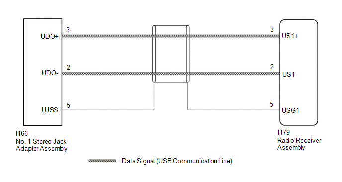
The No. 1 stereo jack adapter assembly sends the sound data signal or image data signal from a USB device to the radio receiver assembly via this circuit.
WIRING DIAGRAM
PROCEDURE
| 1. | CHECK HARNESS AND CONNECTOR (RADIO RECEIVER ASSEMBLY - NO. 1 STEREO JACK ADAPTER ASSEMBLY) |
| (a) Disconnect the I179 radio receiver assembly connector. |
|
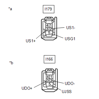
(b) Disconnect the I166 No. 1 stereo jack adapter assembly connector.
(c) Measure the resistance according to the value(s) in the table below.
Standard Resistance:
| Tester Connection | Condition | Specified Condition |
|---|---|---|
| I179-2 (US1-) - I166-2 (UDO-) | Always | Below 1 Ω |
| I179-3 (US1+) - I166-3 (UDO+) | Always | Below 1 Ω |
| I179-5 (USG1) - I166-5 (UJSS) | Always | Below 1 Ω |
| I179-2 (US1-) or I166-2 (UDO-) - Body ground | Always | 10 kΩ or higher |
| I179-3 (US1+) or I166-3 (UDO+) - Body ground | Always | 10 kΩ or higher |
| I179-5 (USG1) or I166-5 (UJSS) - Body ground | Always | 10 kΩ or higher |
| OK | .gif) | PROCEED TO NEXT SUSPECTED AREA SHOWN IN PROBLEM SYMPTOMS TABLE |
.gif)
| NG | | REPAIR OR REPLACE HARNESS OR CONNECTOR |
READ NEXT:
 Mute Signal Circuit between Radio Receiver and Stereo Component Amplifier
DESCRIPTION This circuit sends a signal to the stereo component amplifier assembly to mute noise. Because of that, the noise produced by changing the sound source ceases. If there is an open in the ci
Mute Signal Circuit between Stereo Component Amplifier and Telematics Transceiver
DESCRIPTION This DCM (telematics transceiver) sends a mute signal to the stereo component amplifier assembly. The stereo component amplifier assembly controls the volume according to the mute signal f
AVC-LAN Circuit
DESCRIPTION Each audio system component connected to the AVC-LAN (communication bus) transfers switch signals using the audio visual communication local area network. If a short to +B or short to grou
SEE MORE:
DC / DC Converter Status Circuit Low Input (P0A09-265)
DESCRIPTION Refer to the description for DTC P0A08-264. Click here The hybrid vehicle control ECU sends a signal to the DC/DC converter to prohibit its control and receives signals indicating a normal or abnormal (below 11 V auxiliary battery voltage) condition of the 12 V charging system from th
Seat Heater for Front Left Seat does not Operate
DESCRIPTION When the seat heater switch on air conditioning control assembly is operated, the air conditioning amplifier assembly receives the signal. The air conditioning amplifier assembly receives the signal and operates the front seat heater. WIRING DIAGRAM CAUTION / NOTICE / HINT NOTICE:
If
